Ubiquitous relaxation in BTI stressing-new evaluation and insights. Kaczer, B; Grasser, T; Roussel, Ph.J; Martin-Martinez, J; O’Connor, R; O’Sullivan, B.J; Groeseneken, G. IEEE International Reliability Physics Symposium Proceedings 2008
Our materials growth and processing research develops novel materials and processing methods directed towards applications in high-tech microelectronics, sensing, and sustainability, working in collaboration with key industrial and scientific partners.

About the Research Area
Novel materials coupled with precision processing techniques enable unique functional devices on sub-micron and nanometre length scales. The ability to work at the interface of materials growth and processing, and to utilise a wide variety of processing techniques, including non-equilibrium plasma methods, enables us to access a broad range of parameter space and to develop innovative new materials, composites and structures suited to specific applications. Our wide range of analysis and characterisation techniques provide us with detailed understanding of the scientific basis of the material and device behaviour and these techniques are designed to maximise their relevance to the high-tech manufacturing sector by replicating industrial conditions to give our work maximum impact.
Research Projects
Materials Growth and Processing Publications
In situ H2S passivation of In0.53Ga 0.47As/InP metal-oxide-semiconductor capacitors with atomic-layer deposited HfO2 gate dielectric. O’Connor, E; Long, R.D; Cherkaoui, K; Thomas, K.K; Chalvet, F; Povey, I.M; Pemble, M.E; Hurley, P.K; Brennan, B; Hughes, G; Newcomb, S.B. Applied Physics Letters 2008
Anomalous positive-bias temperature instability of high-k/metal gate nMOSFET devices with Dy2O3 capping. O’Connor, R; Chang, V.S; Pantisano, L; Ragnarsson, L.-A; Aoulaiche, M; O’Sullivan, B; Adelmann, C; Van Elshocht, S; Lehnen, P; Yu, H; Groeseneken, G. IEEE International Reliability Physics Symposium Proceedings 2008
Impact of nitridation on recoverable and permanent negative bias temperature instability degradation in high-k /metal-gate p-type metal oxide semiconductor field effect transistors. Aoulaiche, M; Kaczer, B; Roussel, Ph.J; O’Connor, R; Houssa, M; De Gendt, S; Maes, H.E; Groeseneken, G. Journal of Vacuum Science and Technology B: Microelectronics and Nanometer Structures 2009
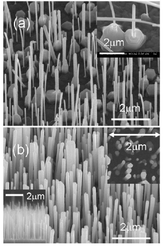
Strong multiphoton-absorption-induced UV luminescence from ZnO nanorod arrays grown by vapour-liquid-solid mechanism. Das, S.K; Bock, M; Biswas, M; Mcglynn, E; Grunwald, R. CLEO/Europe – EQEC 2009 – European Conference on Lasers and Electro-Optics and the European Quantum Electronics Conference 2009

