Experimental
DCU Nano Research Facility
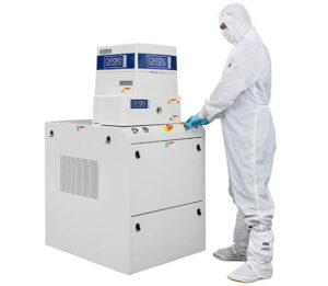
NCPST collaborates with DCU’s Nano Research Facility (NRF). The NRF provides open access high end state of the art scientific equipment for research in academia and industry.
Atomic Layer Deposition
Offerings
- Rapid sample transfer time between Atomic Layer Deposition (ALD) processing module and the X-Ray Photoelectron Spectroscopy (XPS) system. This all occurs under ultra-low vacuum which eliminates atmospheric effects such as oxidation.
- In-situ surface plasma treatments of surfaces
- Optimization of Atomic Layer Deposition (ALD) processes including investigations of infiltration of ALD precursors into polymer materials
- Plasma assisted oxidation/reduction studies of infiltrated polymer materials
- Monochromated XPS based chemical characterisation of individual processing steps.
- XPS 2-D mapping of surface chemical composition at a spatial resolution of 10µm
Ultrafast Spectroscopy
Offerings
- A spectral range of 320-900 nm, which can be extended into the near-IR up to 1600 nm.
- A time delay range of 0-8 ns, with a time resolution of better than 50 fs.
- A delay step size of 2 fs and bi-directional repeatability of 8 fs.
- Sample sizes of up to 200 mm x 250 mm
Offerings
- Modes include Mid-IR Pump with Mid-IR Probe, 2D Mid-IR, UV/Visible Pump with Mid-IR Probe and Transient 2D-IR (UV/Visible Pump with 2D-IR).
- Spectral range of 3-12 µm or 830-3300 cm-1, with a spectral window of 1.5 µm at a centre wavelength of 5 µm.
- In transient mode, the system has a maximum (double pass) delay of 4 ns with a corresponding step size of 16.7 fs.
Hitachi M308 ECR Industrial Etcher
Coming soon
The Hitachi M308 ECR is an industrial etcher, it produces high energetic electrons in the resonance zone which create very dense plasmas at very low pressure. The addition of a low frequency bias source on the wafer results in independent control of plasma density and ion flux. The low pressure operation gives improved directionality of fluxes arriving at the wafer surface. These characteristics significantly influence etching uniformity and speed. Moreover, ECR plasma sources have two frequencies and, in contrast to single frequency plasma sources, are designed for the “independent” control of an ion flux and an ion energy.
Oxford Instrument RIE and CVD 100
Coming Soon
The PlasmaPro 100 RIE modules deliver isotropic and anisotropic dry etching for an extensive range of processes. It is suitable for research and production customers, providing a controlled environment that improves process repeatability with load-lock and cassette-to-cassette options.
- Compatible with all wafer sizes up to 200mm
- Single-wafer or batch processi
ng with excellent process control - High control of the gases and plasma power
- Rapid change between wafer sizes
- Low cost of ownership and ease of serviceability
- Excellent uniformity, high throughput and high precision processes
- In-situ chamber cleaning and end-pointing
- Wide temperature range electrode, -150°C to 400°
Chemical Vapour Deposition (CVD) & PECVD tools for growth of 1D/2D nanomaterials and heterostructures. PlasmaPro 100 Nano (formerly Nanofab) delivers high-performance growth of nanomaterials with in-situ catalyst activation and rigorous process control, with flexible temperatures up to 1,200°C.
- Excellent uniformity with flexible temperatures up to 1200°C
- Options of a 700°C, 800°C or 1200°C table
- Sample sizes up to 200mm
- Vacuum load lock – Quick sample exchange
- Cold wall design with showerhead based uniform precursor delivery
- Optional liquid/solid source delivery system for growth of
- MoS2,MoSe2 and other TMDCs
Oxford Instrument RIE 80
The PlasmaPro 80 reactive ion etch (RIE) is a compact, small footprint system offering versatile etch and deposition solutions with convenient open loading. It is easy to site and easy to use, with no compromise on process quality. The open load design allows fast wafer loading and unloading, ideal for research, prototyping and low-volume production. It enables high performance processes using optimised electrode cooling and excellent substrate temperature control.
- Open load design allows fast wafer loading and unloading
- Excellent etch control and rate determination
- Excellent wafer temperature uniformity
- Up to 200mm wafers
- Low cost of ownership
- Built to Semi S2/S8 standards
Other Facilities
Details coming soon
Details coming soon
Details coming soon
Details coming soon
Details coming soon
Details coming soon
Details coming soon
Details coming soon
Details coming soon
Details coming soon
Details coming soon