Materials Growth and Processing

Our materials growth and processing research develops novel materials and processing methods directed towards applications in high-tech microelectronics, sensing, and sustainability, working in collaboration with key industrial and scientific partners.

About the Research Area

Novel materials coupled with precision processing techniques enable unique functional devices on sub-micron and nanometre length scales. The ability to work at the interface of materials growth and processing, and to utilise a wide variety of processing techniques, including non-equilibrium plasma methods, enables us to access a broad range of parameter space and to develop innovative new materials, composites and structures suited to specific applications. Our wide range of analysis and characterisation techniques provide us with detailed understanding of the scientific basis of the material and device behaviour and these techniques are designed to maximise their relevance to the high-tech manufacturing sector by replicating industrial conditions to give our work maximum impact.

Research Projects

Materials Growth and Processing Publications

Filters
Reset

Zn doped nanocrystalline CuCl thin films for optoelctronic applications. Rajani, K.V; Lucas, F.O; Alam, M.M; Daniels, S; McNally, P.J. Materials Research Society Symposium Proceedings 2010

A study of drop-coated and chemical bath-deposited buffer layers for vapor phase deposition of large area, aligned, zinc oxide nanorod arrays. Byrne, D; McGlynn, E; Kumar, K; Biswas, M; Henry, M.O; Hughes, G. Crystal Growth and Design 2010

A novel, substrate independent three-step process for the growth of uniform ZnO nanorod arrays. Byrne, D; McGlynn, E; Henry, M.O; Kumar, K; Hughes, G. Thin Solid Films 2010

Thermodynamic aspects of the gas atmosphere and growth mechanism in carbothermal vapour phase transport synthesis of ZnO nanostructures. Saunders, R.B; McGlynn, E; Biswas, M; Henry, M.O. Thin Solid Films 2010

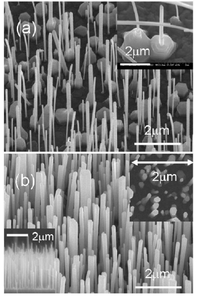
Multi-photon excited UV luminescence of ZnO nanorods after irradiation with few-nJ femtosecond laser pulses. Das, S.K; Byrne, D; McGlynn, E; Bock, M; Grunwald, R. Lasers and Electro-Optics/Quantum Electronics and Laser Science Conference: 2010 Laser Science to Photonic Applications, CLEO/QELS 2010 2010

Adhesion performance of TiN coating with amorphous NiTi alloy interlayer onto 316L stainless biosteel deposited by sputtering process. Abubakar, T; Rahman, M; Dowling, D.P; Stokes, J; Hashmi, M.S.J. Surface Engineering 2010

Electron density, optical emission spectroscopy and fluorocarbon deposition rate measurements in a high density inductively coupled C4F 8 plasma. Kavanagh, D; Goodyear, A; Cooke, M; Daniels, S. 37th EPS Conference on Plasma Physics 2010, EPS 2010 2010

Effects of Ar and O2 additives on photopatternable sol-gel etching in an SF6-based plasma for planar lightwave circuit fabrication. Kolodziejczyk, B; Ellingboe, A.R; Daniels, S; Oksuz, L; Oubaha, M; Barry, H; Copperwhite, R; O’Dwyer, K; MacCraith, B.D. Microelectronic Engineering 2010

Thermal fatigue properties of laser treated steels. Aqida, S.N; Calosso, F; Brabazon, D; Naher, S; Rosso, M. International Journal of Material Forming 2010

Process mapping of laser surface modification of AISI 316L stainless steel for biomedical applications. Chikarakara, E; Naher, S; Brabazon, D. Applied Physics A: Materials Science and Processing 2010

Analysis and prediction of dimensions and cost of laser micro-machining internal channel fabrication process. Shadi, K; Brabazon, D. EPJ Web of Conferences 2010

Development of technique for 3D printed mould intricate rapid casting. Brabazon, D; Kennedy, D; Tyrell, M. 21st Annual International Solid Freeform Fabrication Symposium – An Additive Manufacturing Conference, SFF 2010 2010

Multi-technique characterisation of MOVPE-grown GaAs on Si. Wong, C.S; Bennett, N.S; McNally, P.J; Galiana, B; Tejedor, P; Benedicto, M; Molina-Aldareguia, J.M; Monaghan, S; Hurley, P.K; Cherkaoui, K. Microelectronic Engineering 2011

Characterisation of laser modified WC-CoCr coatings. Chikarakara, E; Punset, M; Picas, J.A; Brabazon, D; Naher, S. AIP Conference Proceedings 2011

High resolution photoemission study of the formation and thermal stability of Mg silicide on silicon. Casey, P; Hughes, G. Thin Solid Films 2011

Laser surface modification of H13 die steel using different laser spot sizes. Aqida, S.N; Naher, S; Brabazon, D. AIP Conference Proceedings 2011

Analysis of microstructural changes during pulsed CO2 laser surface processing of AISI 316L stainless steel. Chikarakara, E; Naher, S; Brabazon, D. Advanced Materials Research 2011

Evaluation of the effect of Nd: YVO 4 laser parameters on internal micro-channel fabrication in polycarbonate. Karazi, S.M; Brabazon, D. NCTA 2011 – Proceedings of the International Conference on Neural Computation Theory and Applications 2011

Interdiffusion and barrier layer formation in thermally evaporated Mn/Cu heterostructures on SiO2 substrates. Lozano, J.G; Lozano-Perez, S; Bogan, J; Wang, Y.C; Brennan, B; Nellist, P.D; Hughes, G. Applied Physics Letters 2011

Chemical and structural investigation of the role of both Mn and Mn oxide in the formation of manganese silicate barrier layers on SiO2. Casey, P; Bogan, J; Lozano, J.G; Nellist, P.D; Hughes, G. Journal of Applied Physics 2011

Synchrotron radiation photoemission study of in situ manganese silicate formation on SiO2 for barrier layer applications. Casey, P; Bogan, J; Brennan, B; Hughes, G. Applied Physics Letters 2011

Photoemission study of carbon depletion from ultralow-carbon doped oxide surfaces during the growth of Mn silicate barrier layers. Casey, P; Bogan, J; Hughes, G. Journal of Applied Physics 2011

Manufacturing and characterization of biodegradable electrospun tri-phasic nanocomposites. Pascu, E; Mcguinness, G.B; Stokes, J. 24th European Conference on Biomaterials – Annual Conference of the European Society for Biomaterials 2011

A systematic study of (NH4) 2 S passivation (22%, 10%, 5%, or 1%) on the interface properties of the Al2 O3 / In0.53 Ga0.47 As/InP system for n -type and p -type In0.53 Ga0.47 As epitaxial layers. O’Connor, É; Brennan, B; Djara, V; Cherkaoui, K; Monaghan, S; Newcomb, S.B; Contreras, R; Milojevic, M; Hughes, G; Pemble, M.E; Wallace, R.M; Hurley, P.K. Journal of Applied Physics 2011

Optimisation of the ammonium sulphide (NH 4 ) 2 S passivation process on In 0.53 Ga 0.47 As. Brennan, B; Milojevic, M; Hinkle, C.L; Aguirre-Tostado, F.S; Hughes, G; Wallace, R.M. Applied Surface Science 2011

Methodologies for sub-1nm EOT TDDB evaluation. Kauerauf, T; Degraeve, R; Ragnarsson, L.-Å; Roussel, P; Sahhaf, S; Groeseneken, G; O’Connor, R. IEEE International Reliability Physics Symposium Proceedings 2011

Time-Dependent Dielectric Breakdown and Stress-Induced Leakage Current Characteristics of 0.7-nm-EOT HfO2 pFETs. O’Connor, R; Hughes, G; Kauerauf, T. IEEE Transactions on Device and Materials Reliability 2011

Reliability of thin ZrO2 gate dielectric layers. O’Connor, R; Hughes, G; Kauerauf, T; Ragnarsson, L.-A. Microelectronics Reliability 2011