Diagnostics and Sensors

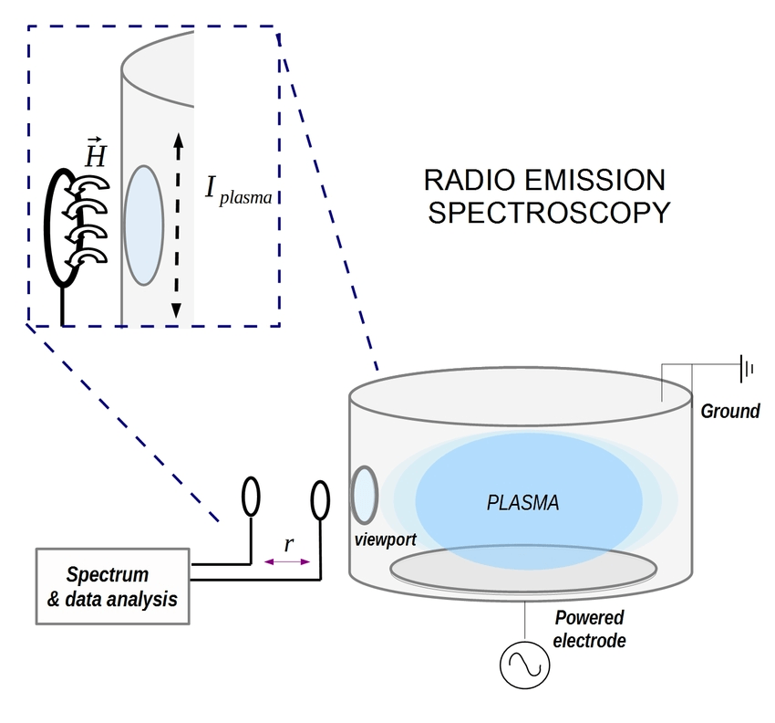
NCPST develops and applies advanced plasma measurement techniques for detailed fundamental investigations as well as smart process monitoring and control technologies.

About the Research Area

Plasma diagnostics are important for measuring and monitoring species, mechanisms and for process control. These, often most powerful when combined with simulations, provide understanding and insight of the plasma environment. This understanding is a key element in the development of plasma control strategies and solutions for technological development. Sensing technologies are important for real time monitoring of processes.
Diagnostics in the plasma environment are not trivial and are under continuous development as knowledge and technology advances. Advanced diagnostic techniques often exploit new laser technologies, coupled with atomic and molecular physics understanding. Electrical plasma emission is also a powerful tool for plasma sensing and process control. Combining sensors or diagnostics with advanced data science techniques can additionally help provide greater insight into complex plasma systems.

Diagnostics and Sensors Publications

Filters
Reset

Nondestructive Monitoring of Die Warpage in Encapsulated Chip Packages. Bose, A; Vijayaraghavan, R.K; Cowley, A; Cherman, V; Varela Pedreira, O; Tanner, B.K; Danilewsky, A.N; De Wolf, I; McNally, P.J. IEEE Transactions on Components, Packaging and Manufacturing Technology 2016

B-Spline X-Ray Diffraction Imaging – Rapid non-destructive measurement of die warpage in ball grid array packages. Cowley, A; Ivankovic, A; Wong, C.S; Bennett, N.S; Danilewsky, A.N; Gonzalez, M; Cherman, V; Vandevelde, B; De Wolf, I; McNally, P.J. Microelectronics Reliability 2016

X-ray asterism and the structure of cracks from indentations in silicon. Tanner, B.K; Garagorri, J; Gorostegui-Colinas, E; Elizalde, M.R; Allen, D; McNally, P.J; Wittge, J; Ehlers, C; Danilewsky, A.N. Journal of Applied Crystallography 2016

Two-photon absorption laser induced fluorescence measurement of atomic oxygen density in an atmospheric pressure air plasma jet. Conway, J; Gogna, G.S; Gaman, C; Turner, M.M; Daniels, S. Plasma Sources Science and Technology 2016

Measurement of deposition rate and ion energy distribution in a pulsed dc magnetron sputtering system using a retarding field analyzer with embedded quartz crystal microbalance. Sharma, S; Gahan, D; Scullin, P; Doyle, J; Lennon, J; Vijayaraghavan, R.K; Daniels, S; Hopkins, M.B. Review of Scientific Instruments 2016

Synchrotron white-beam X-ray topography analysis of the defect structure of HVPE-GaN substrates. Kirste, L; Danilewsky, A.N; Sochacki, T; Köhler, K; Zajac, M; Kucharski, R; Boćkowski, M; McNally, P.J. ECS Transactions 2015

Local strain and defects in silicon wafers due to nanoindentation revealed by full-field X-ray microdiffraction imaging. Li, Z.J; Danilewsky, A.N; Helfen, L; Mikulik, P; Haenschke, D; Wittge, J; Allen, D; McNally, P; Baumbach, T. Journal of Synchrotron Radiation 2015

The geometry of catastrophic fracture during high temperature processing of silicon. Tanner, B.K; Garagorri, J; Gorostegui-Colinas, E; Elizalde, M.R; Bytheway, R; McNally, P.J; Danilewsky, A.N. International Journal of Fracture 2015

B-Spline X-Ray Diffraction Imaging techniques for die warpage and stress monitoring inside fully encapsulated packaged chips. McNally, P.J. 2015 16th International Conference on Thermal, Mechanical and Multi-Physics Simulation and Experiments in Microelectronics and Microsystems, EuroSimE 2015 2015

Non-destructive laboratory-based X-ray diffraction mapping of warpage in Si die embedded in IC packages. Wong, C.S; Bennett, N.S; Manessis, D; Danilewsky, A; McNally, P.J. Microelectronic Engineering 2014

Development of B-spline X-ray Diffraction Imaging techniques for die warpage and stress monitoring inside fully encapsulated packaged chips. Wong, C.S; Ivankovic, A; Cowley, A; Bennett, N.S; Danilewsky, A.N; Gonzalez, M; Cherman, V; Vandevelde, B; De Wolf, I; McNally, P.J. Proceedings – Electronic Components and Technology Conference 2014

Energy resolved actinometry for simultaneous measurement of atomic oxygen densities and local mean electron energies in radio-frequency driven plasmas. Greb, A; Niemi, K; O’Connell, D; Gans, T. Applied Physics Letters 2014

Phase resolved imaging of a repetitive extrusion of hydrogen plasma from a hollow cathode source. Dixon, S; Dedrick, J; Charles, C; Gans, T; O’Connell, D; Boswell, R. IEEE Transactions on Plasma Science 2014

In-process phase growth measurement technique in the fabrication of monolithic porous layer open tubular (monoPLOT) columns using capacitively coupled contactless conductivity. Collins, D.A; Nesterenko, E.P; Brabazon, D; Paull, B. Analyst 2013

Real-time control of electron density in a capacitively coupled plasma. Keville, B; Zhang, Y; Gaman, C; Holohan, A.M; Daniels, S; Turner, M.M. Journal of Vacuum Science and Technology A: Vacuum, Surfaces and Films 2013

Crack propagation and fracture in silicon wafers under thermal stress. Danilewsky, A; Wittge, J; Kiefl, K; Allen, D; McNally, P; Garagorri, J; Elizalde, M.R; Baumbach, T; Tanner, B.K. Journal of Applied Crystallography 2013

X-ray diffraction imaging for predictive metrology of crack propagation in 450-mm diameter silicon wafers. Tanner, B.K; Wittge, J; Vagovič, P; Baumbach, T; Allen, D; McNally, P.J; Bytheway, R; Jacques, D; Fossati, M.C; Bowen, D.K; Garagorri, J; Elizalde, M.R; Danilewsky, A.N. Powder Diffraction 2013

Absolute atomic oxygen and nitrogen densities in radio-frequency driven atmospheric pressure cold plasmas: Synchrotron vacuum ultra-violet high-resolution Fourier-transform absorption measurements. Niemi, K; O’Connell, D; De Oliveira, N; Joyeux, D; Nahon, L; Booth, J.P; Gans, T. Applied Physics Letters 2013

Experiments and modeling of a helicon source. Molvik, A.W; Rognlien, T.D; Byers, J.A; Cohen, R.H; Ellingboe, A.R; Hooper, E.B; McLean, H.S; Stallard, B.W; Vitello, P.A. Journal of Vacuum Science and Technology A: Vacuum, Surfaces and Films 1996

Synchrotron X-ray topographic study of strain in silicon wafers with integrated circuits. Karilahti, M; Tuomi, T; Taskinen, M; Tulkki, J; Llpsanenk, H; McNally, P. Nuovo Cimento della Societa Italiana di Fisica D – Condensed Matter, Atomic, Molecular and Chemical Physics, Biophysics 1997

Examination of the crystalline quality of 200 mm diameter silicon substrates using X-ray topography. Curley, J; McNally, P.J; Reader, A; Tuomi, T; Taskinen, M; Rantamaki, R; Danilewsky, A; Schropp, B. Materials Research Society Symposium – Proceedings 1997

Comparative analysis of synchrotron X-ray transmission and reflection topography techniques applied to Epitaxial Laterally Overgrown GaAs layers. Rantamäki, R; Tuomi, T; Zytkiewicz, Z.R; McNally, P.J; Danilewsky, A.N. Journal of X-Ray Science and Technology 1998

Grazing incidence synchrotron X-ray topography as a tool for denuded zone studies of silicon wafers. Rantamäki, R; Tuomi, T; McNally, P.J; Curley, J; Danilewsky, A. Journal of X-Ray Science and Technology 1998