
Abstract
It is challenging to crystalize a thin film of higher melting temperature when deposited on a substrate with comparatively lower melting point. Trading such disparities in thermal properties between a thin film and its substrate can significantly impede material processing. We report a novel solid-state crystallization process for annealing of high melting point molybdenum thin films. A systematic investigation of laser induced annealing from single pulse to high pulse overlapping is reported upon scanning at fluences lower than the threshold required for the damage/ablation of molybdenum thin films. The approach allows better control of the grain size by changing the applied laser fluence. Atomic force microscopy surface morphology and x-ray diffraction (XRD) analysis reveal significant improvements in the average polycrystalline grain size after laser annealing; the sheet resistance was reduced by 19% of the initial value measured by a Four-point probe system. XRD confirms the enlargement of the single crystal grain size. No melting was evident, although a change in the close packing, shape and size of nanoscale polycrystalline grains is observed. Ultrashort laser induced crystallinity greatly enhances the electrical properties; Hall measurements reinforced that the overall carrier concentration increases after scanning at different laser fluences. The proposed method, based on the aggregation and subsequent growth of polycrystalline and single crystal-grains, leading to enhanced crystallization, has potential to be applicable in thin film processing industry for their wide applications.
Export citation and abstract BibTeX RIS

Original content from this work may be used under the terms of the Creative Commons Attribution 4.0 license. Any further distribution of this work must maintain attribution to the author(s) and the title of the work, journal citation and DOI.
1. Introduction
In recent years, thin film transistors (TFTs) have become a dominant technology for switches and as drivers in flat panel displays. TFTs are fabricated at a low material cost and demonstrated in a wide range of applications such as thin film transistor liquid-crystal displays (TFT-LCDs), organic light emitting displays, flat panel displays, and other electronic device applications. The key advantage of TFT technology is their ability to be manufactured on large substrates at low cost per unit area at low processing temperatures enabling TFTs to be directly integrated on a variety of flexible substrates without affecting the electronic functionality of the circuit [1–3]. Among the metallic materials, molybdenum (Mo) has been used extensively in the thin film electronic industry. In LCDs, the display comprises a matrix of the smallest addressable element called pixels [1]. Individual TFTs control the electric field surrounding each liquid crystal segment to admit the appropriate amount of light to illuminate each pixel [4]. In a molybdenum–aluminium–molybdenum (MAM) or other gold or indium tin oxide (ITO) thin film systems, the Mo thin film serves as source/drain electrodes and for gate metallization of the TFT [5]. The lower Mo layer forms a low resistivity contact to the ITO pixel electrode when compared with the aluminium. Mo thin films provide excellent properties as a diffusion barrier preventing current-driven diffusion. Since Mo exhibits a high melting temperature and a low diffusion constant, it avoids any device failure in TFT-LCDs [6, 7]. In transparent amorphous oxide semiconductors based TFTs, the contact resistance of source/drain electrodes to the semiconductor channel can modify device performance and is influenced mainly by the choice of the source/drain material and the interface properties. Mo is reported to be a good ohmic contact material with a comparatively low contact resistance [8, 9]. Mo serves as a promising electrode material due to its relatively low resistivity of ∼5 × 10⁻⁸ Ω cm, a low work function of 4.3–4.9 eV, high melting temperature (2620 °C) and its limited ability for oxidizing at room temperature [10]. For an improved efficiency of Mo based electrodes and contacts in such applications, it is crucial to use Mo films with enhanced electrical properties. Typically, the deposition parameters are optimized for a favourable growth of Mo microstructures to facilitate the requirement of high conductivity for efficient charge transfer in addition to chemical inertness and strong adhesion to the substrate. This is done by using either RF or DC magnetron sputtering techniques or electron beam evaporation followed by an annealing process [11–14]. Unfortunately, thermal annealing processes are not often suitable for localized heating since the higher temperatures can damage/melt the underlying substrates. This problem arises due to high melting temperature of Mo which makes it challenging to anneal Mo on a substrate with low melting temperature, e.g. glass and polymers. Therefore, it is crucial to develop a general solution by lowering the processing temperature for Mo applications in flexible electronics.
In past years, the use of lasers has been demonstrated effectively from material removal to material processing by cutting, drilling, ablating, and crystallization [15–17]. As a promising platform for material processing, lasers offer a precise and localized energy transfer to the material in a well-controlled fashion with repetition rates up to MHz attainable. For example at low repetition rates, an excimer laser of 248 nm wavelength and 24 ns pulse duration, is reported to anneal Mo microstructures for 3D complementary metal-oxide semiconductor (CMOS) compatible with micro-electromechanical system (MEMS) integration [18]. The use of excimer laser annealing with a 30 ns pulse duration is also reported to form Ohmic Mo/Ti contacts to diamond; an alternative to rapid thermal annealing to avoid oxygen diffusion into the contact system [19]. In laser material interactions, processes dramatically change when the pulse duration of a laser becomes ultrashort (⩽picosecond) to cause a non-linear phenomenon. Compared with longer pulse durations (millisecond to nanoseconds), ultrashort pulses are characterized by their high peak power and pulse durations much smaller than the major electron-lattice relaxation processes [20]. A recent report on clean material ablation demonstrates the use of IR femtosecond laser pulses for selective ablation of Mo film from aluminium in a commercial heterostructure (MAM) thin film system without melting the aluminium layer underneath [21]. In ultra-short laser metal interactions, free electrons in a metallic system absorb laser energy and heat up within few femtoseconds (fs) due to the small heat capacity of electrons. These excited electrons then thermalize and transfer their energies to the lattice system determined by an electron–phonon coupling factor. This two-step non-equilibrium energy transfer was proposed by Anisimov et al and is referred to as two temperature model (TTM) [22] and was later modified by Chen and Beraun who considered the lattice heat conduction and hence provided a more accurate lattice temperature [23]. The concept of the TTM phenomenon is utilized in the current study where we optimized the laser fluence to work below the damage threshold. By doing so, we process thin films with a range of single to multiple laser pulses to selectively crystallize the Mo thin films. The study reported here is new in its nature and provides a possible solution for thin film annealing using ultrashort laser pulses where we demonstrate how a fs laser can be used to better align and grow polycrystalline grains thus enabling selective crystallization of a high melt temperature Mo thin film without deteriorating the underlying substrate. A number of studies have been recently reported for ITO [24], silicon [25] and gold thin films [26], respectively. It was revealed that the degree of crystallinity exhibits a wavelength dependency and is strongly influenced by the laser wavelengths as observed in gold thin films using IR, green and UV laser pulses [26]. For silicon, it was demonstrated that the use of an additional metal layer could enable a larger process parameter window for semiconductors compared to processes where one is not used [25]. For ITO, the process demonstrated simultaneous enhancements in the electrical conductivity and optical transparency of an oxide semiconductor [24]. This paper provides new information on the nano-scale evolution of the grain structure during ultrashort laser induced crystallization which is possible to observe in high melting temperature Mo films.
2. Experimental details
An industrial grade 40 nm Mo thin film was deposited by magnetron sputtering on a 500 nm thick layer consisting of Si (30 nm) and SiO2 (470 nm) which in turn is deposited on a glass substrate of 500 µm thickness. A femtosecond laser (s-Pulse HP Amplitude systems) of pulse duration 500 fs, at a wavelength of 515 nm which can operate from single pulse to 300 kHz was used to improve Mo crystallization. The laser is focused with a telecentric f-theta lens of 100 mm focal length. The sample position was controlled using a high precision 3D computer-controlled stage (Aerotech 3200). A galvanometer XY scanning system (SCANLAB, hurry SCAN II) controls the pulse to pulse overlap on the sample. The polarization state was changed by a half-wave plate placed before the scanning system. The schematic diagram of experimental setup is shown in figure 1. The Van der Pauw method was used to measure the sheet resistance of Mo film before and after the laser scanning with a commercial Four-Point Probe System (Ossilla UK). To observe the effects of different laser fluences on the charge carrier mobility and concentration, the Hall measurements were also performed before and after laser treatment by using the Ecopia Hall Effect Measurement system (HMS-3000). Atomic force microscopy (AFM) and scanning electron microscopy (SEM) are utilized to analyse surface morphology before and after laser irradiation. The crystallinity of the Mo films was quantified using a triple-axis Jordan Valley Bede D1 high resolution x-ray diffraction (XRD) system using a Cu-Kα (λ = 1.5405 Å) radiation source operated at 45 kV and 40 mA. XRD measurements were carried out in grazing incidence geometry with an incident angle of 3° with a step size of 0.1°.

Figure 1. Schematic diagram of crystallization experiment for femtosecond laser setup.
Download figure:
Standard image High-resolution image3. Results
Figure 2 presents the plots showing a linear relationship between the squared diameter  and natural log of (a) laser energy and (b) fluence, respectively. The laser spot diameter at the focused position
  was calculated experimentally using the Liu method, given by the following relation [27];
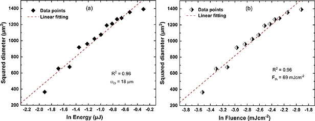
Figure 2. Linear relationship between squared diameter and (a) log of energy and (b) log of fluence to determine laser beam waist radius and threshold fluence for 40 nm thick Mo films, respectively.
Download figure:
Standard image High-resolution imagewhere  is the measured diameter of the crater,
  is beam waist radius of the Gaussian shaped beam at the focus,
  is the pulse energy and
  is the threshold energy, respectively. The beam radius is calculated from the slope of the graph between
  and the log of energy (figure 2(a)). The estimated
  for 515 nm laser wavelength is 18 µm ± 0.11 µm. The absorbed threshold fluence
  is calculated by considering the reflection and transmission of green wavelength for Mo [28]. The fluence at which Mo film starts to peel off from the underlying surface, is defined as the damage/ablation threshold
  and have calculated from the equation below [27];
After single pulse irradiation, a fluence of 69 mJ cm−2 is estimated as the damage threshold fluence for 40 nm Mo thin film as seen by AFM and optical microscopy.
3.1. Polycrystalline grain microstructures
To explore the single pulse laser induced effects, Mo thin films were irradiated at different laser fluences of 36 mJ cm−2, 47 mJ cm−2 and 55 mJ cm−2. A comparison of surface topography using AFM of as-deposited Mo thin films with laser treated films at different fluences is given in figure 3. The as-deposited Mo surface is composed of irregular dense particles or polycrystalline grains of approximately 90 nm in size and are not well-defined in shape. When the film was exposed to laser pulses, no apparent damage was seen on the Mo film surface. However, we observed a change in the morphology of the film. The surface morphology of the as-grown Mo film is shown in figure 3(a). The AFM scanned area of 3 µm × 3 µm is selected randomly from 9 mm × 9 mm Mo thin film samples. At the fluence of 36 mJ cm−2, the randomly orientated irregularly-shaped particles converted to a more uniform spherical-like geometry and reconfigured into a close packed structure (figure 3(b)). The average particle size at 36 mJ cm−2 is improved from 90 ± 2.97 nm to 110 ± 2.86 nm, respectively. The value of surface roughness (Sq ) of unexposed Mo film is 1.79 ± 0.05 nm that increases to 2.08 ± 0.13 nm after irradiating at 36 mJ cm−2 fluence. At an increased fluence of 47 mJ cm−2 (figure 3(c)), a compacted film of larger and diversely shaped particles or truncated spherical grains emerged. The average particle size increases to 180 ± 4.97 nm and the surface roughness improves to a value of 2.85 ± 0.32 nm. When the fluence was increased further to a higher value of 55 mJ cm−2, the particle size increased to a value of 288 ± 11 nm with 3 ± 0.22 nm surface roughness; here the grains are no longer spherical in shape. It can be observed that the number of grain boundaries have reduced significantly, and they are well connected at this stage by forming a smoother film surface (figure 3(d)). It is evident from AFM images that the average particle size has improved after fs laser irradiation. When the experimental evidence from the three fluences is considered together, the results suggest that no melting was observed, instead the growth of grains occurred due to a solid-state diffusion process.

Figure 3. Mo thin films (a) before laser treatment and after single shot crystallization at (b) 36 mJ cm−2, (c) 47 mJ cm−2 and (d) 55 mJ cm−2 fluence, respectively. The surface line profiles are added below each AFM image.
Download figure:
Standard image High-resolution image3.2. Effect of laser annealing on electrical properties
The evidence of grain growth in Mo thin films using a single femtosecond pulse have been clearly realised in the AFM surface topographic images (figure 3). Surface morphology and the electrical properties are interconnected for many grains across the laser treated thin films. To study the fs laser induced effects on electrical properties, a commercial Four-Point Probe System was used to measure the sheet resistance before and after laser irradiation. To enable this electrical measurement, a laser treated area needed to be created on the Mo material. The Mo thin films were scanned at higher pulse to pulse overlapping at fluences significantly lower than the damage threshold (69 mJ cm−2). The samples were scanned at 180 mm s−1 laser scan speed and 100 kHz repetition rate with a spot size of 36 µm which resulted in 20 shots per area and 95% overlapping of the consecutive pulses. The laser scanning parameters and fluence values are optimized to avoid any melting and visible damage on the Mo surface. Figure 4 exhibits the variation in sheet resistance measured before and after each laser scan. The sheet resistance of as-deposited 40 nm Mo thin film was measured as 5.29 ± 4.74 × 10⁻³ Ω Sq−1. The sheet resistance was reduced to 4.81 ± 3.79 × 10⁻³ Ω Sq−1 after scanning at a single pulse fluence of 22 mJ cm−2 in such a way that the whole area of 9 mm × 9 mm Mo thin film sample was treated using 6 µm hatching; the distance between two consecutive laser scans. Upon scanning with slightly higher fluence of 25 mJ cm−2, the sheet resistance dropped to 4.77 ± 1.65 × 10⁻³ Ω Sq−1 and became 4.52 ± 2.85 × 10⁻³ Ω Sq−1 at further higher fluence of 29 mJ cm−2. When the fluence was increased to a value of 32 mJ cm−2, and the film was re-scanned, the sheet resistance dropped to 4.42 ± 2.59 × 10⁻³ Ω Sq−1. At the highest scanning fluence of 34 mJ cm−2, the sheet resistance reduces to 4.27 ± 1.71 × 10⁻³ Ω Sq−1 which resulted in a 19% improvement in conductivity. Using fluences higher than 34 mJ cm−2 causes the on-set of damage therefore we marked this as the effective threshold fluence at 100 kHz repetition rate.
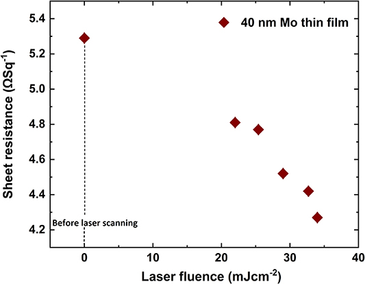
Figure 4. Decrease in sheet resistance as a function of absorbed laser fluence in an optimized regime before and after 515 nm laser scanning of 40 nm Mo thin film.
Download figure:
Standard image High-resolution imageWe also investigated the effect of scanning at a direct single laser fluence value on another sample . Upon directly scanning at 34 mJ cm−2, the sheet resistance decreases from 4.96 ± 2.21 × 10⁻³ Ω Sq−1–4.19 ± 1.71 × 10⁻³ Ω Sq−1 giving a 15.5% improved conductivity; lower than the improvement achieved when the Mo film was scanned starting from a lower value with a gradual increase in fluence below the onset of damage. To explore further, we raised the fluence higher than the value used previously (34 m−2) to 36 mJ cm−2 and attained a decrease in sheet resistance by 14%, which is lower than the other values achieved. From these observations, we summarize that starting with a lower fluence with a gradual increase and keeping below the threshold is the best practice to obtain significant improvements in conductivity.
Laser treatment can also vary the other electrical properties of the material, for example the mobility and the charge carrier concentration. The mobility is a sensitive parameter that depends on the particle size. Hall measurements are performed to see the effect of laser irradiation on mobility and the carrier concentration at different laser fluences (figure 5). Initially, at 22 mJ cm−2, the mobility increases from 3.49 cm2V−1 s−1 to 3.69 cm2 V−1 s−1 where the carrier concentration increased from 7.95 × 1022 cm3 to 9.43 × 1022 cm3, respectively. The mobility was observed to increase to a value of 4.86 cm2 V−1 s−1 up to the fluence of 34 mJ cm−2 and reduces again to 4.15 cm2 V−1 s−1 at the highest fluence of 36 mJ cm−2. It is worth noticing that the mobility is still greater than the initial value (3.49 cm2 V−1 s−1). The mobility of the Mo film is influenced by the continuity of the film structure and is related to electron–phonon scattering in the thin film, especially at the grain boundaries. On contrary, the carrier concentration of the Mo film is mainly the concentration of the free electrons and was less influenced by possible free electron trapping at the varied sizes of grain boundaries established under different laser fluences. The carrier concentration of Mo film may also be partly influenced by electron diffusion from Mo to the substrate. At the highest fluence of 36 mJ cm−2, the carrier concentration increases to a value of 8.53 × 1022 cm3 which is higher than the untreated Mo thin film. Hall data support the sheet resistance results; higher mobilities are compensated with lower charge carrier concentration where the higher carrier concentrations are balanced with a reduced mobility and vice versa.
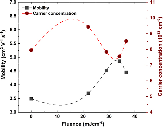
Figure 5. The variation in mobility and carrier concentration in laser annealed Mo thin films at different laser fluence. Dash lines are a visual aid only.
Download figure:
Standard image High-resolution imageSEM characterization was carried out to investigate the variations in the grain size after scanning at 100 kHz repetition rate. Figure 6 shows the SEM images of the surface structure of Mo thin film after scanning at 22 mJ cm−2 and 32 mJ cm−2 fluence. The irregular grains composed of tiny sub-nanometre sized particles are transformed into the spherical well-defined grains of 70 nm ± 5 nm size at a fluence of 22 mJ cm−2 (figure 6(a)). The enhancement in the grain size is significant and it increases to a value of 120 ± 8 nm when the fluence is increased to 32 mJ cm−2 (figure 6(b)). The almost same surface morphology was observed at the next higher laser fluence of 34 mJ cm−2 and film start to damage as a result of surface cracking with further increasing fluence. SEM images provide a good measure of surface structures after annealing Mo films at higher pulse to pulse overlapping. The variations in the morphology of Mo film after laser annealing may further explain the results of change in mobility of Mo film as shown in figure 6. It is observed that the grain size increases with increasing laser fluence and results in reduced electron scattering leading to a higher mobility in the Mo film. The bigger grains increase the electron mobility within the Mo grains, while the gaps between the grain boundaries could decrease the charge mobility of the overall Mo film. The competition between the two effects leads to the decrease of charge mobility of Mo film again when the fluence of the laser is too high.
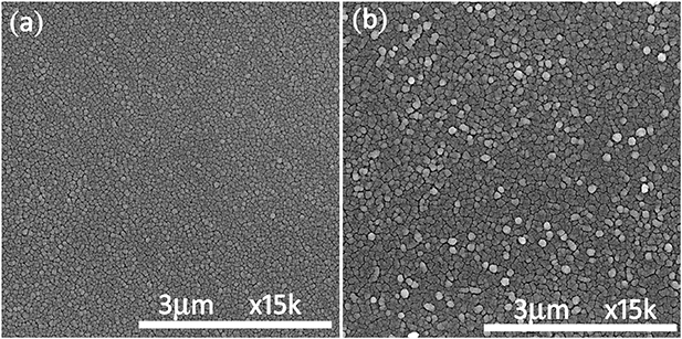
Figure 6. SEM images revealing the surface morphology of 40 nm Mo film at (a) 22 mJ cm−2 and (b) 32 mJ cm−2 laser fluence, respectively.
Download figure:
Standard image High-resolution image3.3. Effect of crystallinity on single crystallite size
XRD is an excellent technique that provides information about crystal structure, phase, and crystallinity of the material. XRD gives a good estimation of the crystallite size which is sensitive to any change in the full width at half maximum (FWHM) of the diffracted peaks in XRD spectrum. The crystallite size is directly related to the FWHM of XRD peaks and a reduced FWHM after laser treatment confirms increased crystallite size [26, 29]. To investigate if there is any change in phase occurred due to laser annealing, XRD analysis in the Bragg-Brentano mode was carried out on the untreated and laser treated Mo films (figure 7). It is observed that the Mo films maintain a body centred cubic crystal structure and figure 7 indicates the presence of the major peak at 2θ = 40.30° with the for a scattering configuration in the (110) direction in reciprocal space. Two minor peaks labelled (200) and (211) are also evident at 2θ angles of 58.60° and 73.50°, respectively. The sharp peak at 57° (blue asterisk) corresponds to the (311) peak from the silicon substrate, which often appears during grazing incidence XRD, as the Si (311) scattering configuration can be detected for x-rays at grazing angles. Gaussian-Lorentzian curve fitting was used to acquire the peak position and FWHM of the (110) peak. A reduction of 10.5% and 31% in FWHM of (110) peak is obtained after laser scanning at 32 mJ cm−2 and 34 mJ cm−2 fluence, respectively. A slight peak shifting toward higher 2θ angles was observed which is possibly due to a change in lattice parameters or relaxation of internal compressive stresses (strains) after laser annealing which were established during thin film deposition process [24]. The Scherrer equation is used to estimate the size of the nano-crystallites as [30];

Figure 7. XRD diffractograms of unexposed and laser exposed Mo thin films of 40 nm thickness scanned at 32 mJ cm−2 and 34 mJ cm−2 fluence, respectively.
Download figure:
Standard image High-resolution image
where  is the crystallite size,
  is FWHM at diffracted angle (
 ). The estimated crystallite size increases from approximately 12 nm to 14 nm at 32 mJ cm−2 and, to 18 nm at 34 mJ cm−2 laser fluence, respectively (table 1). There were improvements in conductivity after laser treatment at low fluence (22–29 mJ cm−2) but no significant enhancement in crystallite size was observed at these fluence values. The instrumental broadening factor is considered in our calculation of crystallite size. The XRD results confirm the crystallinity is enhanced in laser scanned thin Mo films. The estimated crystallite sizes are in agreement with our AFM measurements of multi-grain particle sizes; the AFM measurements suggest that the grains are larger and may consist of multiple crystals. XRD confirms that single crystallite size is increased as a result of fs laser induced crystallization.
Table 1. XRD peak analysis of untreated and laser treated Mo thin films and the corresponding crystallite size estimation.
| (110) peak | |||
|---|---|---|---|
| FWHM | Peak position (2θ°) | Crystallite size (nm) | |
| Unexposed | 0.728 | 40.30 | 12 |
| 32 mJ cm−2 | 0.651 | 40.65 | 14 |
| 34 mJ cm−2 | 0.502 | 40.81 | 18 |
4. Discussion
Low fluence controlled enhanced crystallization of Mo thin films in a multi-layered structure is demonstrated. It is challenging to selectively process a high melting temperature thin film on an underlying layer with a comparatively lower melting point. Ultrashort laser processing of a thin film with a very high melting temperature was carried out after optimizing the process window parameters and selecting the best optimized value including laser fluence, repetition rate (100 kHz), scan speed (180 mm s−1) and hatching (6 µm). The exciting part of this work lies in the fact that the Mo films were treated at very low fluence to avoid any damage or melting as higher powers can fully melt the crystal lattice followed by a cooling and a re-solidification process resulting in enhanced grains. The results show that Mo can be selectively crystallized at a fluence lower than its melting temperature using single pulse and at higher pulse overlapping. Before considering the physics behind the crystallization process, it is essential to understand the ultrashort laser material interaction. When an ultrashort laser is focused on the metal surface, the photon energies are mainly absorbed by the conduction band electrons through photon–electron interaction as the electron heat capacity is typically orders of magnitude lower than the lattice [25]. Since Mo is a transition metal with electronic structure (4d5 5s1), the conduction electrons in the  -band absorb the incident laser energy [31]. This leaves the electronic subsystem into an excited state and the lattice remains unperturbed. After a few fs, the electrons re-establish the Fermi–Dirac distribution during a characteristic time called electron relaxation time required by the electrons to restore their states [25, 32]. Initially the excited electrons are localized within the optical penetration depth
  (∼10 nm for green wavelength) and diffuses into the deeper parts of the film due to large temperature gradients in the electron and lattice systems. At picosecond timescale, the electron–phonon interactions transfer the thermal energy of the electronic system to the lattice by means of electron–phonon coupling. The higher the value of the electron–phonon coupling factor, the faster the rate of energy transfer to the lattice will be thus establishing an equilibrium in the thin film system.
We investigated the fs laser induced enhanced crystallinity in two ways, (a) with single pulse and (b) a large area scan with multiple pulses at 100 kHz repletion rate. Upon irradiation with a single laser pulse, enhanced crystallization of the Mo thin film was observed without any visible damage to the surface or to the substrate underneath. The laser associated parameters greatly impact the crystallization process. Since the absorption length of the laser (10 nm) was smaller than the film thickness, the laser beam did not propagate deep into the 40 nm thick film thus avoiding any damage to the substrate. The AFM images in figure 3 clearly show the degree of grain or particle enlargement with the increasing fluence. Results suggest the particles coalescence to create closer packed and bigger grains/particles by a solid-state diffusion process. No evidence of melting was observed on the topography, neither was there any other visible damage on the film. This increase in particle size after laser exposure reduces the number of grain boundaries which results in the reduced scattering of electrons. Up to 19% improved crystallinity (from a fourpoint probe) has been achieved upon scanning the Mo samples at 180 mm s−1 below the damage threshold fluence. Hall measurements confirm the increased mobility and carrier concentration after laser treatment, which is also fluence dependant revealing an overall improvement in the electrical properties of laser annealed Mo thin films. XRD characterization reveals a decrease in FWHM of the main diffraction peaks for the laser scanned Mo films, and these confirm that crystallite size increases with increasing fluence. We suggest this enhancement in overall particles size after fs laser annealing is not due to melting and re-solidification, rather it occurs due to a solid-state crystallization process. As described earlier, when ultrashort laser irradiates the Mo surface, electrons are excited first due to their smaller heat capacities. These electronic excitations can vary the electron density distribution in the solid giving rise to modified interatomic forces [33]. As a result, the modified interatomic forces create coherent atomic motion and structural transitions on a very short time scale (sub-picosecond). Such transitions occur without electron to phonon energy transfer and are known as non-thermal phase transitions [33]. We suggest that the enhanced crystallization after laser annealing occurs due to non-thermal solid-state diffusion of atoms in interstitial sites at a local scale of nanometres. This work reports improved electrical conductivity of high melting temperature Mo films in a controlled low fluence regime with minimal thermal damage to the underlying layers. This approach can be adopted for a melt-free enhanced crystallization of very thin films for improved practical applications in everyday industry.
5. Conclusions
We investigated a low temperature laser annealing method to modify the crystallization process of Mo thin films with single pulse and by scanning with highly overlapped fs laser pulses without affecting the underlying SiO2-glass layers. Our process leads to significant improvement in both polycrystalline and single crystal grain size with improved electrical conductivity. Hall measurements confirm an overall improvement in the mobility and carrier concentration in laser treated Mo thin films. XRD suggest an increase in the crystal size in addition to better compaction and enlargement of grains. We suggest that the selective non-melt crystallization occurs due to a solid-state diffusion process where the process fluence was well below the damage threshold. The process offers up to 19% decrease in sheet resistance of 40 nm Mo thin films enabling their future, better use in flexible electronics. The approach is also significant for optimising the structure of nanoparticle coatings on heat sensitive substrates.
Acknowledgments
The authors gratefully acknowledge the SEM facility provided by The Centre for Microscopy and Imaging at NUI Galway and their support and assistance in this work.
Data availability statement
All data that support the findings of this study are included within the article (and any supplementary files).
Funding sources
This publication has emanated from research supported in part by a grant from Science Foundation Ireland under Grant Number 16/RC/3872. For the purpose of Open Access, the author has applied a CC BY public copyright license to any Author Accepted Manuscript version arising from this submission. Gerard M O'Connor's contribution and facilities are also supported by EU INTERREG project EAPA 384 2016, 'AtlanticKETMED'.